



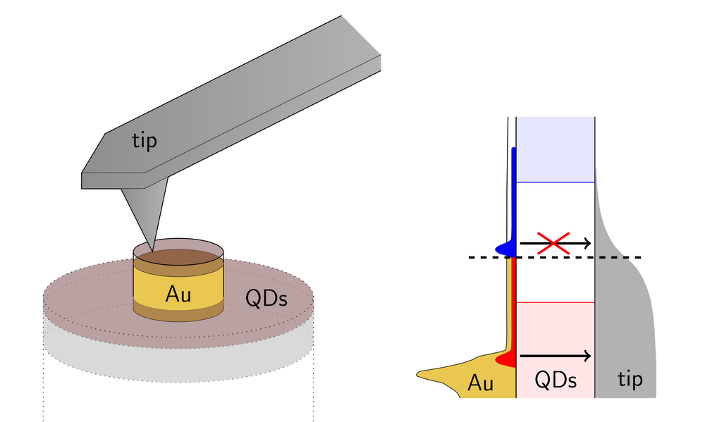
The Nanooptics team of the Physics institute, together with collaborators from ETH Zürich, has developed a new microscopy technique to quantitatively measure the energy distribution of hot charges generated by plasmon decay in individual metal nanoparticles. Plasmons – collective oscillations of conduction electrons in metals – can decay to create highly energetic (“hot”) electrons and holes. These carriers are central to emerging concepts in photocatalysis, photodetection and solar energy conversion, yet direct, energy‑resolved measurements have been largely missing. The new study, published in Nano Letters, closes this gap by turning a monolayer of colloidal quantum dots into an ultrathin, energy‑selective filter that probes which charges, at which energies, can escape from plasmonic nanoparticles.
The experimental scheme is based on a Schottky junction built on a single nanoparticle. A plasmonic gold or aluminum nanoparticle acts as the bottom electrode and hot‑carrier source. On top of this, Ph.D. student Florian Küstner succeeded in depositing a monolayer of lead sulfide quantum dots, provided by the ETH partners. The tailored dots provide a bandgap and band alignment that allow only carriers above a certain energy to cross. A conductive atomic force microscope tip forms the top electrode. When the nanoparticle is illuminated, only specific carriers can pass through the quantum dot layer to reach the tip, where the resulting photocurrent is measured. By combining systematic parameter variations including wavelength control, Florian Küstner separated the hot carriers from other current contributions and thereby accessed the energy‑filtered hot carrier population. As a specific example, the hole population from gold in the energy range of 1.9-2.6 eV was reported.
Beyond this specific demonstration, the method is broadly applicable. By changing the quantum dot material and size, the bandgap can be tuned to select different energy windows and carrier types, allowing the same detection scheme to be applied to hot holes as well as hot electrons in different energy ranges. Because the technique relies on a scanning probe scheme, it combines nanometer‑scale spatial resolution with energy selectivity, offering a powerful new tool for fundamental hot‑carrier spectroscopy and for the rational design of plasmonic metal–semiconductor interfaces in photocatalysis, photodetection, and photovoltaics.
F. Küstner, H. Ditlbacher, A. Hohenau, D. N. Dirin, M. Kovalenko, J. R. Krenn, Quantum-dot-based scanning probe d‑band hole spectroscopy of plasmonic nanoparticles, Nano Letters 26, 14040 (2026), https://doi.org/10.1021/acs.nanolett.6c03990